OSSD, Open Source Solenoid Decoder


Welcome to my webpage over the OSSD. On this page you’ll find a complete tutorial for ordering a fully soldered DCC decoder for solenoids, signals and other accessories.

As most model railway enthiusiasts know, these kind of decoders are expensive and often cost over €60,-. Well now you get to buy ‘em directly at the source for roughly 1/6th of that price.

I’ll explain how the decoder works and how you can configure and use it in your modelrailway layout.

I will also explain in great details how you can order this decoder directly at the PCB manufactoring plant of JLCPCB. It is by far the cheapest PCB service in the world and they offer excellent quality.

Than I’ll explain how you can program the board with my software turning a lifeless PCB into a fully functional DCC solenoid decoder.

This entire project is 100% open-source. You are free to do with it whatever you want: study, modify, distribute, make, and sell the design. Do so under the licences of the below links.

Link to OSHWA
Link to GPL v3

Index


  1. Commissioning
    1. Signals, outputs and addresses explained
      1. Outputs
      2. Addressing
    2. Connecting
    3. Configuring
      1. Set DCC Address
      2. Configure outputs
      3. Configuration Mode
      4. List of supported signal types and aspects
  2. Ordering
    1. Step 1: Download the necessary files.
    2. Step 2: Open Google Chrome and surf to JLCPCB
    3. step 3: upload the gerber files and adjust a setting or two
    4. Step 4: Select your BOM and CPL
    5. Step 5: Pick your components.
    6. Step 6: Verify component positions
    7. Step 7: Put the PCB in your basket and make the purchase
  3. Finish soldering
  4. Programming the OSSD
    1. Make the connections
    2. Flash the ArduinoISP program
    3. Flash the OSSD
  5. Schematics
  6. Source Code
  7. Consider a small contribution
  8. Contact

Commissioning


I’ll first explain how to the decoder works and how you can use it.

Signals, outputs and addresses explained


Outputs

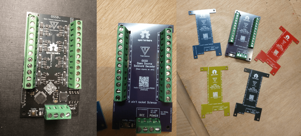
The OSSD is an DCC accessory decoder. It has 16 outputs with which it can switch a numerous amount of accessories. One such accessory or object as I like to call them can be anything. It can be a point motor, it can be a signal, a relay, a smoke generator etc. You can use different kinds of objects on a single OSSD.

The OSSD was originally designed to control point motors but it happens to do a decent job at other items as well. By default all outputs are configured for 8x point motors. And the OSSD will switch with a 100ms pulse

Every object needs a certain amount of outputs. A point motor needs two, a relay need only one and some signals may even use up to eight outputs. Depending on what kind of objects you configure, the total amount of objects may be different. If you only use single output objects, you will have 16 objects. If you use 3 signals with 5 outputs each you will have 3 objects and a spare output.

The OSSD puts the objects’ outputs automatically in a sequential order. If the first object uses 5 outputs, than the second object’s outputs start at the 6th output. This safes you from configuring the output numbers yourself.

Addressing

Every object has one or more DCC addresses, regardless of outputs. You can configure the start address yourself. Like with the outputs, the OSSD will also correctly assign DCC addresses to all objects in a sequential order.

Some objects like signals often need more than one DCC address. Some signals have nice or even more different aspects to show. For every two aspects one DCC address is needed. So if the base address is ten, and the first object uses five DCC addresses than the second object will start at address fifteen.

It is however also possible to configure a unique address per object if desired.
Likewise it is also possible to use only one DCC address per object using the DCC EXT protocol. I myself find it convenient to group signals per five addresses like 10, 15, 20 etc.

Bear in mind that the amount of outputs and the amount of DCC addresses are not related to eachother. A single output object has 3 aspects, that is ON, OFF and blinking. Therefor it needs 2 DCC addresses per object. So if you configure 16 outputs all as single output objects, the OSSD will use 32 DCC addresses. But if you use 8 point motors which have 2 outputs and 1 address each, the OSSD will use only 8 DCC addresses.

Connecting


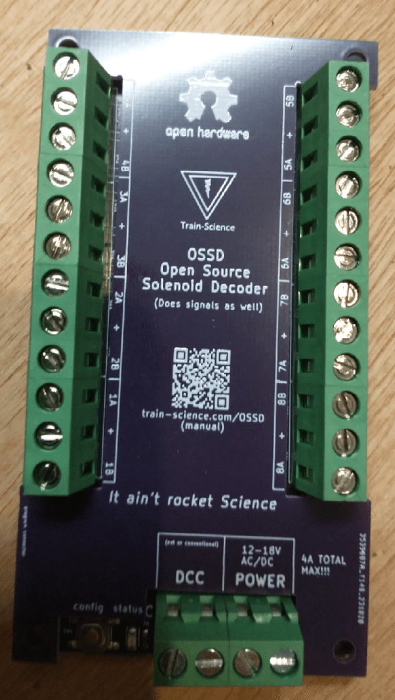
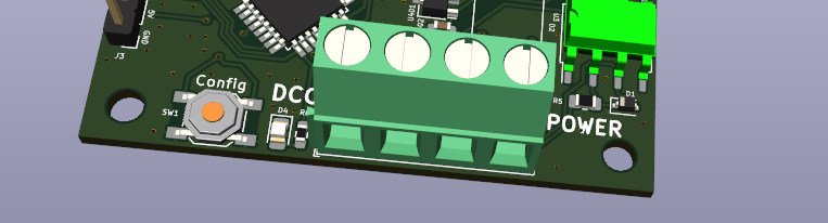
Connecting the board to your modelrailway is fairly simple. The 4P screw terminal has 2 connections for the DCC wires on the left. And 2 connections for power (AC or DC) can be inserted on the right.

I do not recommend using DCC as power source. If the the DCC bus is turned off, the OSSD will forget the states of all his objects. For point motors this does not matter. But if a train causes a short, al your signals will show their default aspect when they are turned on again.

Connecting your point motor is also fairly simple. The decoder has 8 of these connectors. You just put the three wires of your point motor in the screw terminal. The middle wire is the common lead.

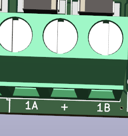
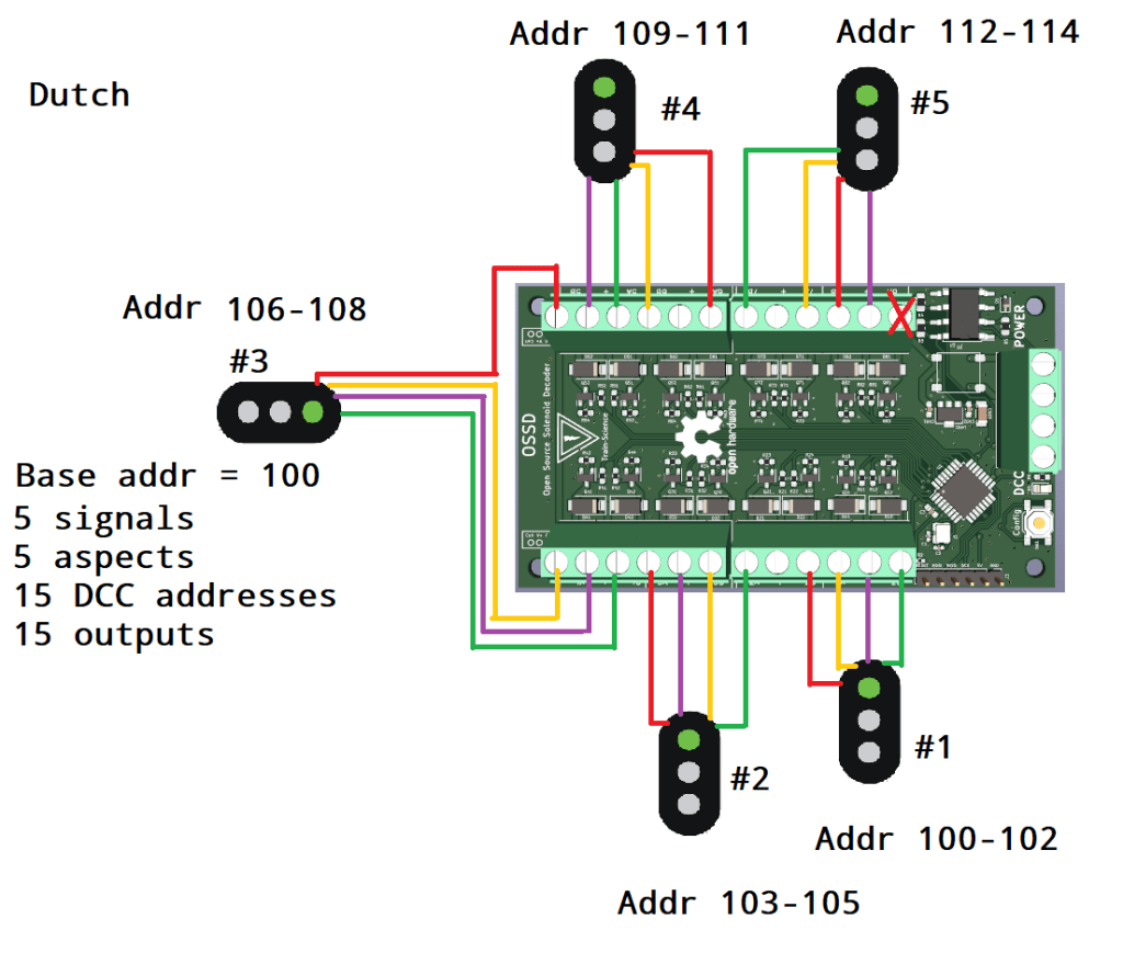
If you use signals with more than 2 outputs, you need to use sequential outputs. Take note that 1B counts as the first ouput and 1A as the second. By this order 2B is the third output 2A is the fourth output, 3B is the fifth etc.

I tried to maintain a certain order in connecting a signal from green to stop. Below are the numbering of the signals. The numbers indicate the order. The order must be maintained from low to high.

You can zoom in on the PDF below if needed.

A connection example of 6 german signals. The orange wires are the + leads of the the signals. Also take note how the DCC addresses are divided and how al the objects are wired.

Example UK 4-tone signals with point indicator
Example Dutch block signals, with number indicators.

Configuring


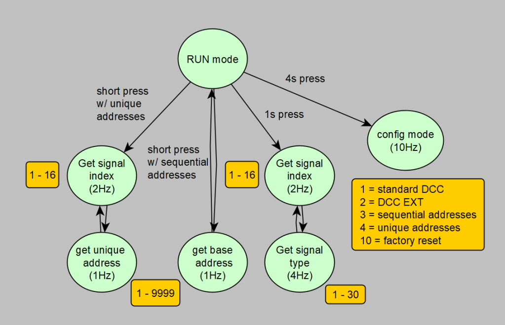
The decoder is easily configurable with the dedicated config button and hand-held throttle. Inserting a number is done by setting a DCC point using your hand-held throttle. It does not matter which in direction you set a point

By giving a short press you can configure the address

With a longer press of one second you can configure the outputs. You can configure the outputs to act as your average double coil driver or as one of the many different signal types.

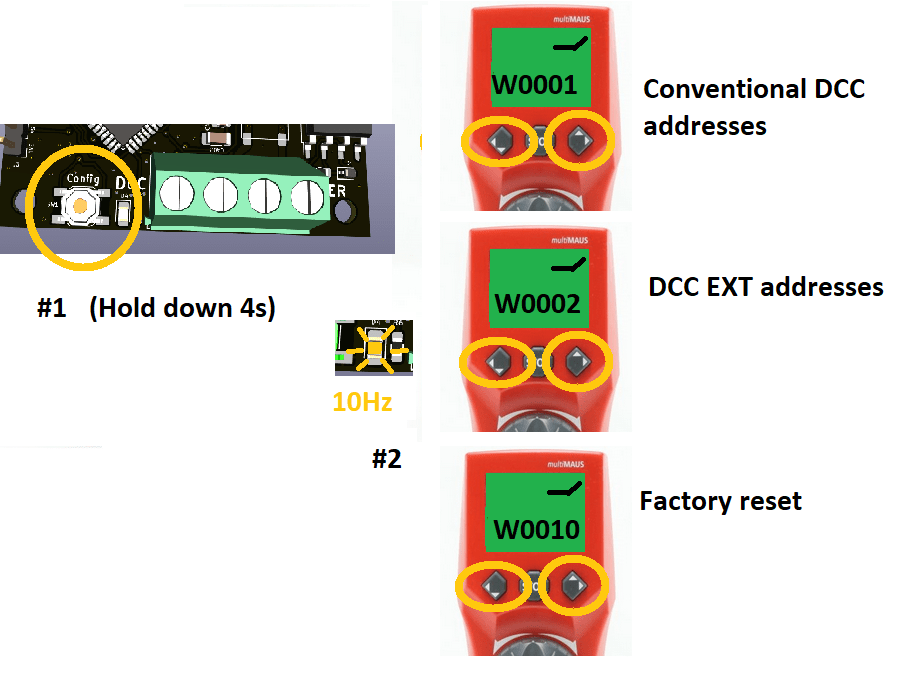
If you hold down the button for 4 seconds you can enter the the configuration mode. In this mode you can choose between normal DCC and DCC extended messages and you get to chose between sequential addresses or unique addresses per item.

Below there is a flow chart of the config menu. It may help you understand the configuration process.

Set DCC Address


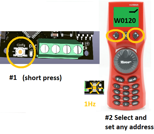
With a short press on the config button you can put the OSSD in ‘get address mode’. How this works depends if you use unique addresses per signal or sequential addresses (default).

In case of the latter the decoder will listen for the first DCC accessory address. In this mode the LED will blink at 1 Hz. The received address will be coupled to it’s first object. All other objects will get sequential addresses assigned automatically. After the base address is assigned the decoder jumps back to idle/run mode.

In case of unique addreses the LED blinks slightly faster at 5Hz. You first need to select which of the signals is going to get a new address. You can select a signal by setting the appropiate address. When you have selected the signal the LED will blink at 1Hz which means that the OSSD is ready to receive an address.

When you have configured the address the OSSD is immediately ready to configure the next signal. At this point the LED blinks again at 5Hz. This allow you to configure all addresses relative quickly. If you are finished with configuring all addresses you can simply press the config button again and the OSSD goes back to idle/run mode.

Example of setting DCC address 120 as first DCC address.

Configure outputs


By holding down the config button for 1 full second (you can see this when the LED flashes) will allow you to configure the outputs. There are many different presets to chose from. By default the double coil mode for point motors is active.

The LED will flash at 2Hz. At this point you need to select which of your objects (object being a point, single output or signal) you want to configure. You can select a object by setting a point with your throttle. If you set point 1 you wil be able to configure the first object. If you set point 2 you can configure the 2nd object etc.

After you have selected your object, the LED will flash at 4Hz. Now you need to pick the output type or signal type. You need to look up in the table which signal type you want to use. You need to set a switch again with the corresponding address. So if you want to select signal type #4 you just have to set point #4 and that is it.

An example. You just configured the first signal. For the 2nd signal you want to use the the 5th signal type. First you press and hold the configure button for 2 seconds. Than you set point #2 to indicate that you you are configuring the second object and than you can set point #5 directly afterwards.

After having configured an output, the OSSD leaves config mode and you have to press the config button again for 2 seconds to configure another output.

I highly recommend to first write down on a piece of paper what you want to configure. This will make the actual configuring more easy. And you have an oversight of the the used outputs and used DCC addresses. The former is important for wiring the OSSD and the latter is important for configuring your computer program for the correct aspects.

Here follow a few examples of different configuration possibilities.

Example of German signals
Example dutch block signals

This last example has something interestings. The last 2 outputs are not connected, but they are in use. By default there is still a double coil point motor configured and the outputs will still be controlled whether something is connected or not. You can simply not connect anything and use the address for an other decoder. Or perhaps you want to use the free outputs to control the station or street lighting. You are ofcourse free to configure the 6th and 7th object to be single output devices.

Configuration Mode


If you hold down the configuration button you can enter the configuration mode. There are only two configurations you can alter. With the DCC addresses 1 and 2 you can disable and enable DCC extended commands respectively. With the the addresses 3 and 4 you can choose between sequential or unique addresses respectively.

The DCC extended protocol will allow you to use just one address per signal. With the extended protocol various aspect numbers can be transmitted under a single address.

By default the OSSD squashes the addresses in a sequential order. You can however give every signal it’s own unique address. This can be usefull if a certain light needs to follow the position of a point. It also allows you to apply a certain order to your own liking.

If you use address 10 you will put the OSSD in factory defaults.

Note. Point motors will always work under conventional DCC addresses. So you can connect signals and point motors to one OSSD, have the signals working under DCC EXT and the points under conventional DCC.

List of supported signal types and aspects


Here follows a list with all different objects types and their aspects. The first three types aren’t signals however. The 1st type is a regular point motor, the 2nd is a single output device and the 3rd type is a dutch AKI.

For every type it is listed how many outputs, aspects and DCC addresses they use. If you spot an error or miss something, please fill in the contact form (and preferbly with a suggestion fix).

This chapter concludes the configuration process. If you have done everything by the book, your OSSD should be fully operational.
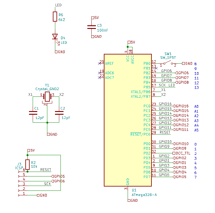
Ordering


Ordering a bare PCB @ JLCPCB is incredibly simple. To make use of the SMT assembly service takes some efforts. I therefor made a guide how to make use of their SMT assemble services.

disclaimer: Be aware that ordering my design is at your own risc. If you screw something up and get defective boards don’t look at me.

Step 1: Download the necessary files.


Click on this link to download a zip file for this project. This include the gerber files, Bill Of Materials and a Component Placing List. These are files you need to order the PCB and make use of JLCPCB’s SMT assembly service. The files lie in the PCB folder.

N.B. it seems that the above link tends to raise security flags. You can find all files here https://github.com/bask185/Train-Science-DIY/tree/master/PCB/DECODERS_N_OCCUPANCY/OSSD. In order to download the entire folder. You need to download the entire Train-Science-DIY repository. https://github.com/bask185/Train-Science-DIY/tree/master click on the green code button and click download ZIP.

Once the zip file is downloaded, extract it.

Step 2: Open Google Chrome and surf to JLCPCB


The website is sometimes updated and I found that this may come with bugs from time to time. It is therefor imperiative to use the Google Chrome browser for the following steps. So no edge, safari or firefox. Surf to JLCPCB.com and create an acount. You can also login with your Google acount. You will need an acount for ordering PCBs. Having an acount also makes it easier to repeat previously made orders.

step 3: upload the gerber files and adjust a setting or two


Gerber files are files which contain the physical properties and infomation about the PCB design itself. They are needed to order PCBs. They are stored in a zip file. This zip file you need to upload

Uploading the gerber files can be done by clicking on the ‘add gerber files’. A window will pop-up. Navigate to your newly downloaded folder and click on the zip files which is named GERBERS.zip.

This will lead you to the next screen on JLCPCB.com. There are alot of settings there but you only need to touch a few of them.

You need to select the amount of boards you want to order. JLCPCB has a cheap and more expensive service. With the cheap service you can order up to 50 assembled PCBs. Ordering 50 boards will give you a fairly low price per unit.

The absolute minimum number is 5. If you order 5 you have a special option to do SMT assembly on only 2 of them. Bear in mind that this will increase the price per unit. More boards -> less $ or € per board

The most important setting of all. Select your color!! You are free to order any color of choise. However anything else but green and black will be more expensive for SMT assembly. Black also takes slightly longer to be produced. So that may cost a day or three more. With black you may order 30 units max (for economic service) if you pick green you can order up to 50. Otherwise you may use the more expensive service.

The last setting you need to do is to select SMT assembly. It is somewhere at the bottom of the screen. Also make sure that you select top side behind the ‘assembly side’ setting if itsn’t selected already.

I also recommend to check ‘Yes’ behind Confirm Parts Placement. This wel let their personal double check your work. And it only costs a few cents.

Lastly, by default JLCPCB places an order number in silk on your board. You can set a setting behind ‘Removed Order Number’ to prevent JLCPCB from doing so. This costs a few cents as well.

If you press Next you get to the next screen. This one only wants to know if you want to do the top or bottom side. It should already say top side, so can just press next.

Step 4: Select your BOM and CPL


Here you need to upload two more files. That is the Bill Of Material (BOM) and the Component Placing List (CPL), Click on the zones where you see upload and select the appriopate files from your downloaded folder. They are named BOM and CPL and are hard to miss. Press Next when you are finished.

Press ‘Process BOM & CPL when you are ready.

Step 5: Pick your components.


If I did my job properly you won’t have to do anything at all, besides pressing Next. In this page you can select parts and search for them. This information is already in the BOM you just uploaded. So you can just hit Next and go to step 6.

For the sake of clarity I will explain a few things. JLCPCB has ‘basic’ parts and ‘extended’ parts. Basic parts are already in their assembly lines. Extended parts need a roll with components to be swapped by hand. A fee of 3$ is charged for this. This project only contains one extended part and that is a 4 Ampere bridge rectifier.

In the bottom of the list the components are placed which don’t have components. In our case that is every screw terminal. (I’ll exclude them from the BOM in the future)

In absolute worst case scenario it may occur that a component is out of stock. I did check stock amounts when I picked the components. So with a little luck it shouldn’t ever happen.

Were it to happen, you can try to search for a replacement part or what perhaps is easier, is to purchase the missing component somewhere like Aliexpress and solder it by hand. (soldering SMD is really not that hard). I picked relative large components. Or you can give me a call and I may find a replacement part for you.

Step 6: Verify component positions


In this step we need to visually examine our board design and our component placing.

This is what you should see. At first I had a problem with the rotations of some components and you would have to rotate and drag a few components. This problem has been corrected. And you shouldn’t have to do anything in this step. I do recommend to visually check everything. See if it looks okay.

When you are sure about the component places, click on Next.

Step 7: Put the PCB in your basket and make the purchase


For some dark reason you need to enter a product description on the right side. I usualy select ‘other’ and ‘other’ again and then I type something like ‘model railway’ but it does not really matter.

If all above steps are completed without any errors. You are ready to place the order. Do so now. Click on save to cart and don’t back down. You are almost there!

The final thing you can do, is to alter the amount of PCBs you want to order. Yes you already did this before and now can change your mind and buy even more PCBs. I do have bad experiences with altering the number. It often does not work. Even on Chrome. If you are ok with the quantity, click on ‘secure checkout.

On the next screen you just need to fill in your adres. With an acount JLCPCB will remember this for the next time. So fill everything in and hit continue.

You will see that the shipping is sorta expensive. However you are able to select much cheaper shipping services. Take note that you are also charged with an import fee as well taxes. This is good as this usually result in no customs related problems and unexpected import costs. So far I have not experienced any problems with customs when ordering stuff from JLCPCB.

The glocal standard direct line is often cheapest (and slowest). However it often takes like 1.5 week livery.

As you can see, for 5 PCBs you have to pay around €56,-. So every board is around €11. If you purchase 50 boards, you will pay around €5 per board*. A commercial equivalent is easily €60+.

If you made a new acount you may also make use of a coupon for your first order.

So just complete the purchase and … well just wait for it.

If you are happy with your decoder and you want to order more for personal or commercial purposes, you can easily re-order the boards using the order history @JLCPCB. You don’t have to repeat the above steps for this.

So feel free to manufactor them and sell em on.

Shipping costs note


*While testing an order with 50 units. The cheap shipping (Global Standard Direct Line) service was not available. There was one relative cheap service but that one did not cover taxes and import. So I believe that that one would get you into trouble with customs.

The more expensive shipping was a whopping €100 more expensive. For 50 boards I would have to pay a grand total of ~€340 which is roughly €6,80 per board. The boards themselfes actually cost only €210.

I checked with JLCPCB and the tipping point is an order of $150,-. So try to keep batches under $150,- I haven’t figured out how many PCBs that exactly are. Propably 25 or 30 pieces. This will get you relative cheap shipping with import and tax fees taken care of.

Finish soldering


JLCPCB does offer the option to hand or wave solder the screw terminals. The screw terminals are in 5.08mm pitch. This does involve manual labour and therefor increases manufactoring costs. I have not tried this myself. I also could not find screw terminals I liked.

N.B. I have removed the screw terminals from the BOM

It is not that expensive but it will always remain cheaper to do it yourself. It should take no more than 10 minutes of your time, 3 if you’re quick.

You can just insert all terminals in the board, flip the board upside down. Solder all terminals like in the picture. I recommend to solder one pad first and make sure that the terminal is firmly pressed against the board. If necessary reflow the pad and press the terminal against the board.

One really important node about screw terminals. Aliexpress is filled with these ones among others. They suck to put wires in without ferrules. DO NOT BUY THESE. I can know I have like 200 of those things…

Look for these ones instead. You can find them here among others. The decoder needs 2x 12P connectors (you can couple 2 6P to make a 12P) and 1x a 4P (or 2x a 2P). Pay attention that the pitch is 5.08mm. Not 5.00mm!! You can also look for slightly more expensive ones at your local electronics shop or webshop.

You should definatetly safe money by buying these DIY decoders but you should not safe money on the screw terminals. Or you will be screwed (pun intented)

The soldering is real easy. The first thing you need to do is to shuff the screw terminals into eachother until you have 1 12P long block. You also need to use a 1P block for the Power and DCC connections.

Than put the terminals in the designated positions. Make sure that the wire opening side is aimed outside.

N.B. that the revision PCB has the 2×6 closer togahter in 1×12 arrangement. This require you to string all 4 headers in eachother. You can also look for 6P of even 12P terminals. They do exist.

Turn the board around and solder all contacts. And needless to say, do work straight. It looks better that way 😉

Programming the OSSD


Programming the OSSD has to be done via a method which is called In Circuit Serial Programming or ICSP for short. The Arduino website has a very elaborate explanation how that works and how you can do this. I have a shorter tutorial however.

Make the connections


The OSSD cannot be connected to a computer directly. In order to do this we need to use an Arduino board.

The first thing we must do is, is to make the connections between Arduino and OSSD. Make sure that the Arduino is not plugged in the computer while you connect the wires.

The OSSD has an ICSP connector for programming. In order to connect the wires. I recommend that you solder a conventional pin connector on it. The pins are marked so it should be easy to hook it up to an arduino. You can simply use depont wires for this. You need to make the following 6 connections

Connections to make
ICSP connector of the OSSD
OSSD connected to the Arduino programmer.

When the Arduino is connected to the OSSD you can plug it in the computer via an USB cable.

If you intend to do this often you may consider buying a 1×6 pogo pin clamp. With it you don’t have to ‘do’ the wires and solder the program connector. This clamp has conical pins which are pressed against the program connector with a spring.

Flash the ArduinoISP program


The second thing we need to do is turn this Arduino board into a programmer by flashing Arduino’s ‘ArduinoISP’ program into the board. When that is done we can use the Arduino board to program the OSSD.

For both programming the Arduino and OSSD there is the easy way and the slightly less easy way. The easy way is as simple as clicking on “upload_ISP.bat” in the software folder.

This will open a window which prompts you for a COM port number. You can find all attached COM ports in the windows device manager. Looks for something that says something like CH340 or FTDI.

Enter the COM port number and hit Enter. If all goes well you should see the following.

This was the easy way. 2 mouse clicks and 2 button presses.

The less easy way involves downloading and installing the Arduino IDE on your computer. It is a fairly simple process you can just surf to arduino.cc, click “software” and navigate down to Arduino IDE 1.8.19

Once installed you need to open the example sketch named ArduinoISP and flash it into the Arduino board.

Open ArduinoISP sketch in the IDE

Make sure to set the COM port and board settings right. You can see which COM ports are available in the IDE. It is usually the bottom one. Set board type to UNO (or NANO depending on what you bought)

Set Board and COM port settings right.

Finally click on the upload arrow.

Arduino UNO being programmed as ICSP programmer

When the Arduino is programmed it is almost ready to be used as programmer. You need to put in a capacitor in the Arduino (10uF or more). The long leg (+) should go in the reset pin and the short pin (-) should go in a GND pin. This capacitor prevents the Arduino from being reset when we try to program the OSSD.

Added capacitor

Once you have succesfully programmed the Arduino board with the ISP program, made all the proper connections and inserted the capacitor, the programming of the OSSD can now commence!

Flash the OSSD


Like before there is the easy way and the slightly less easy way. Again the easy way exists out of double clicking “upload_OSSD.bat” in the software folder and entering the COM port number. If that goes well you should see a similar result as before.

With the Arduino IDE method, you need to do 2 steps. Before you program the board with the OSSD program, you’ll first need to burn the bootloader. This is also explained on the Arduino website. It is however incredibly simple… You can just click on ‘Tools’ and ‘burn bootloader’. Also make sure that board and COM port settings are correct.

Extra information: The bootloader is usually needed for an arduino to allow programming via USB. However it is also important because it sets the Atmega’s fuse bits to work with the correct clock frequency. If you don’t do this the decoder will operate at 1/16 speed and won’t be able to do decode a single DCC message.

When the bootloader is ‘burned’ you must open the OSSD project in the Arduino IDE. You can do this from within the IDE itself via ‘File’ -> ‘Open’. Or you can navigate to the src\SOFTWARE\OSSD folder in the explorer and double click OSSD.ino. This should open the IDE for you with the program open.

Double click OSSD.ino

This is what you should see now.

OSSD.ino opened in the IDE

In order to program the OSSD program into the OSSD we won’t be using the conventional upload method with the arrow. You need to tell the IDE that we will be using an Arduino as ISP programmer. You can do so by clicking on ‘Tools’-> ‘Programmer’-> ‘Arduino as ISP’.

Than you you must click on ‘sketch’ and ‘Upload Using Programmer’. Or simply hit the shortcut Ctrl + Shift + U.

Doing so will let the Arduino IDE first compile the program and flash it into the OSSD. If you see this message in the bottom of the IDE.

It means that you have a fully operational point motor and signal DCC decoder in your hands. Take note that this process takes around up to 30 seconds.

Schematics


These are are kicad schematic for the DCC decoder. I made use of hierarchial labels and schematic sheets. I’ll explain a little something per sheet.

The root schematic exists out of a uController (atmega328), a DCC decoder circuit, a voltage regulator with rectifier and mosfets to control the solenoids.

solenoidDeocder.kicad_sch (root schematic)

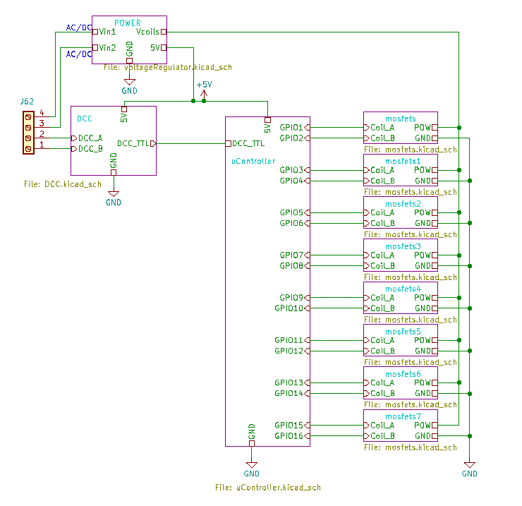
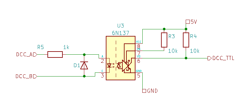
The DCC signals are insulated from the rest of the electronics. I use a 6N137 optocoupler because it is fast enough and is a basic part @JLCPCB.

DCC.kicad_sch

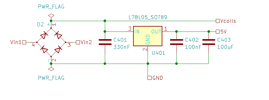
In order to control the point motors. You should use an external power supply. You could use the DCC lines but I don’t recommend this as I have no CDU circuit. The current drawn by your point motors may let your DCC central to go in short circuit. And it is likely you will see all trains’ light flicker.

I use a 5V voltage regulator to supply 5V to the 5V circuit. The incomming power may be either DC or AC. The voltage is rectified and supplied to the coils. The rectifier is limited to just 2A. The total current should not exceed this limit for a long period of time. It should however be safe to switch solenoids of 3A as the switch time is relative short.

In the event that the rectifier dies there are solder pads on the bottom of the board with which you can bypass the rectifier. This does require you to use a DC voltage source.

voltageRegulator.kicad_sch

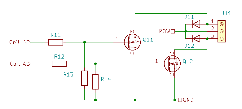
The coils are switched using AO3400A N-channel mosfets. The mosfets are protected with flywheel diodes. The gates are equiped with pulldown resistors and rush-in-current limit resistors. The mosfets are rated to 5.7A max. So they should suffice for most point motors.

mosfets.kicad_sch

The uController is an atmega328. It is equiped with a 16MHz crystal, LED, config switch and a ISP program connector.

uController.kicad_sch

Source Code


The program is not really big nor complicated. I’ll explain briefly what it does. If you want to tinker anything, be my guest. If you do not care about software at al I recommend to skip this chapter.

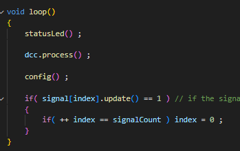
The main loop() of the program only calls a few functions. There are functions for the status led, DCC handling and the configuration menu.

The bottom part keeps updating all signals and or point motors. The if-statement there ensures that in double solenoid mode, only 1 output is activated at any given time to prevent an overload.

The dcc.process() function handles all received DCC packetts. If a valid packett is received, one of two callback function can be called. There is one for an extended protocol packet and one for a regular DCC packet.

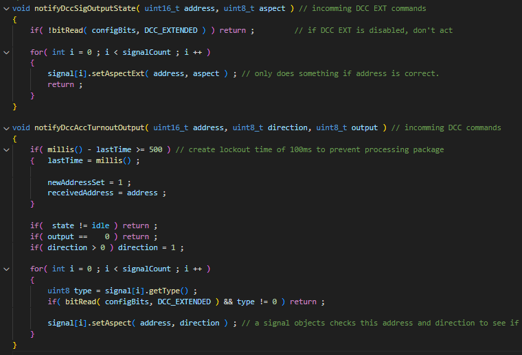
These functions channel the received addresses and direction to the signal objects. The object will determen if they should act on the packett or not.

The variables newAddressSet and receivedAddress are channeled to the config menu. These are responsible for configuring the OSSD.

In an other file name “signal.cpp” you will find a large table with all signal aspects. They should correspond with the PDF on this page. If you want to add or change signal aspects you can do so here. The letter X means blinking. The blinking interval can be calculated with the following formula. If blinking is not used, the value does not matter, you may enter NA if you like.

blinkTime = 3000 / Blinks_per_minute ;

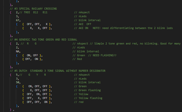
If you make changes, make sure that you maintain the order. All {} and , must be kept clean. It is important that you fill in correct numbers for LEDs and aspects.

Consider a small contribution


Making PCBs like I do isn’t cheap. And DIY projects like this consume alot of time. I have many many more designs I’d like to order and manfactor for you. And I could really use some new decent soldering tools.

If you liked this tutorial, are a happy customer or you simply like what I am doing, please consider supporting me by buying me a cup of coffee. I promise you that every penny will be put to good use.

Contact


If you are in need af anything, have some constructive feedback, would like to order a couple of OSSDs (€34,99), have an idea of your own with which you need some help, miss a certain signal type or have a question, please don’t hesitate to fill in the contact form. And you can ofcourse also leave a message on the bottom of this web page.

Plaats een reactie

Blog op WordPress.com.